
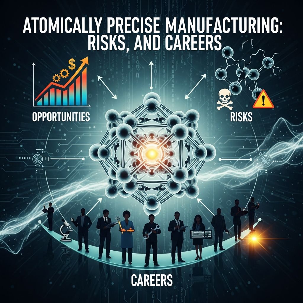
Atomically precise manufacturing (APM) aims to build materials and devices by positioning individual atoms and molecules with near-perfect control. It sits at the intersection of nanotechnology, quantum devices, and advanced manufacturing, and could eventually reshape industries, economies, and global power — for better or for worse.
This article explains what APM is, why it matters, how it might become dangerous, and what kinds of work could help steer it toward beneficial outcomes.
1. What Is Atomically Precise Manufacturing?
In conventional manufacturing, we sculpt matter from the top down: we cut, etch, or print bulk materials into smaller structures. In atomically precise manufacturing, we instead build from the bottom up by arranging atoms and molecules into exactly specified configurations.
1.1 Key ideas behind APM
- Atomic-level control: Every functional part of a device — wires, active elements, interfaces — is defined with near-atomic accuracy.
- Programmable fabrication: Structures are not merely grown but programmed, analogous to software-controlled manufacturing, potentially enabling complex 3D architectures.
- Defect minimization: Many extraordinary material properties emerge only when defects and disorder are reduced to extremely low levels.
- Integration with existing platforms: Early APM efforts focus on familiar substrates such as silicon, diamond, and other semiconductors to leverage existing electronics infrastructure.
1.2 Current technical approaches
Modern research does not yet realize the full vision of general-purpose atomically precise factories, but several methods demonstrate important components:
- Scanning probe methods (e.g., scanning tunneling microscopes) can remove or place individual atoms on crystal surfaces, enabling demonstration devices like single-atom transistors.
- Hydrogen depassivation lithography on silicon can pattern atomically precise dopant arrays, forming ultra-small electronic circuits and quantum devices.
- Atomically precise molecular clusters and nanocarbon structures are synthesized as building blocks for catalysts, sensors, and energy applications.
- Self-assembly in solution or on surfaces uses molecular recognition to form precise patterns, sometimes refined by external fields or templates.
These approaches remain lab-scale, expensive, and specialized, but they illustrate how atomic precision can deliver novel device behavior and performance.
2. Why Could APM Be So Transformative?
If APM scales beyond bespoke laboratory devices to robust, high-throughput production, it could change what we can build, how we build it, and who controls key capabilities.
2.1 Potential technical and economic impacts
- Ultra-efficient electronics: Devices built from atomically precise dopant networks and quantum structures could surpass the limits of conventional semiconductor scaling, enabling new generations of low-power computing and sensing.
- Novel materials: By precisely tuning composition and structure, APM could create materials with combinations of strength, weight, thermal conductivity, or optical response that are unattainable today.
- High-performance catalysts: Carefully engineered active sites can dramatically increase catalytic selectivity and lifetime, improving chemical manufacturing, energy conversion, and recycling processes.
- Energy and resource efficiency: Better catalysts, lighter and stronger materials, and low-loss electronics could reduce energy use across industries and extend the useful life of products.
- Localized production: In the longer term, programmable nanoscale factories could shift some manufacturing from large centralized plants to smaller, highly automated facilities, potentially altering global supply chains.
2.2 Comparing conventional and atomically precise manufacturing
| Feature | Conventional manufacturing | Atomically precise manufacturing (aspirational) |
|---|---|---|
| Primary control scale | Micron to millimeter | Individual atoms and molecules |
| Defect density | Low but significant; limits many properties | Extremely low; properties dominated by design, not defects |
| Material efficiency | Substantial waste from cutting, etching, and scrap | Potentially near-net or net-additive assembly |
| Minimum feature sizes | Set by photolithography and machining limits | Set by atomic spacing and chemistry |
| Design flexibility | Constrained by bulk material properties | Possible to engineer properties via structure and composition |
3. Strategic Risks from Advanced APM
Because APM is so powerful in principle, some scenarios in which it becomes widely available could be extremely dangerous. Even if these scenarios remain speculative, thinking about them in advance may help guide safer research and governance.
3.1 Military and dual-use concerns
Many enabling technologies for APM — advanced nanofabrication, quantum devices, and high-precision catalysts — are heavily relevant to military and intelligence applications. Some potential issues include:
- Next-generation weapons systems: Atomically precise materials could yield lighter and more resilient armor, more efficient propulsion, ultra-sensitive surveillance systems, or highly optimized explosives and guidance components.
- Strategic instability: If a small group acquires a large advantage in manufacturing precision and throughput, it could shift the balance of power in ways that encourage arms racing or pre-emptive conflict.
- Covert production: Compact, high-throughput nanoscale fabrication systems might make it easier to hide prohibited weapons development or bypass export controls.
3.2 Economic disruption and concentration of power
In optimistic scenarios, APM boosts productivity and reduces waste across many sectors. However, the transition could still be turbulent:
- Automation shocks: Fully automated, high-precision nanoscale production could displace large numbers of workers in manufacturing, logistics, and resource extraction.
- Intellectual property bottlenecks: If a small set of entities control crucial APM patents, process know-how, or key equipment, they could extract large rents and slow beneficial diffusion.
- “Winner-takes-most” dynamics: Early technological leads in APM might compound over time, reinforcing global economic inequality and limiting access to advanced capabilities.
3.3 Catastrophic misuse scenarios
Some long-term speculative scenarios involve general-purpose nanoscale factories capable of producing a wide range of products, including dangerous ones. While these capabilities are far from current reality, they motivate early work on safeguards and governance frameworks.
Concerns sometimes raised include:
- Mass production of advanced weapons by non-state actors if compact fabrication platforms become easy to acquire and repurpose.
- Uncontrolled self-replicating systems in which nanoscale devices can copy themselves faster than they are contained, although current scientific and engineering challenges make such systems remote with today’s methods.
- Large-scale environmental damage if extremely efficient nanoscale extraction or processing technologies are deployed without adequate oversight.
These possibilities highlight the value of pairing technical progress in APM with anticipatory policy, safety research, and norms development.
4. Trajectories and Uncertainties in APM Development
Forecasting APM is difficult. The path from prototype atomic-scale devices to widely deployed manufacturing platforms will likely be long and uneven, with bottlenecks in instrumentation, automation, materials, and economics.
4.1 Near-term outlook (next few decades)
On current trends, several developments appear plausible within the next few decades:
- Expanded use of atomically precise dopant placement in specialized semiconductor and quantum devices.
- Automated STM-based systems that pattern surfaces with higher throughput and lower operator involvement, especially for metrology and prototype fabrication.
- Broader industrial adoption of atomically precise catalysts in selected chemical processes, improving efficiency and reducing waste.
- Integration of machine learning to optimize nanoscale assembly pathways and interpret complex imaging data.
These advances are likely to be incremental but important, enhancing certain industries rather than transforming manufacturing as a whole.
4.2 Long-term possibilities
Further out, if key challenges are solved, more radical possibilities emerge:
- General-purpose nanoscale fabrication systems able to assemble a wide variety of structures by following digital blueprints.
- Highly integrated “productive nanosystems” where small, programmable units work cooperatively to build large, complex products.
- Widespread localization of high-end manufacturing, reducing dependence on global supply chains for many advanced goods.
The timing and feasibility of these developments remain highly uncertain. Progress could stall on fundamental engineering issues, economic viability, or regulatory constraints.
4.3 Key open questions
- Will approaches based on scanning probe tools and surface chemistry scale, or will entirely new paradigms be needed?
- How quickly will automation and parallelization reduce costs enough for broader industrial adoption?
- Which fields — electronics, catalysis, structural materials, medicine — will first see large-scale benefits from atomic precision?
- Can governance and safety frameworks evolve fast enough to handle dual-use implications?
5. High-Impact Career Paths Related to APM
Because APM intersects with multiple emerging technologies and potential global risks, there are many ways skilled people might contribute to making its development safer and more beneficial.
5.1 Technical research and engineering
Technical work can both advance APM and help clarify what futures are realistically on the table.
- Nanoscale fabrication research: Developing new patterning methods, improving scanning probe reliability, or inventing scalable self-assembly strategies.
- Quantum and semiconductor device engineering: Using atomic precision to create new sensors, qubits, or ultra-dense classical logic, while building in security and safety features.
- Atomically precise catalysis: Designing catalysts that improve energy efficiency and environmental outcomes in heavy industry.
- Metrology and standards: Establishing robust techniques to verify atomic precision, device reliability, and process reproducibility, which can underpin future regulation and certification.
5.2 Policy, governance, and international coordination
Given the dual-use character of APM, thoughtful governance will be essential. Potentially impactful roles include:
- Science and technology policy in governments or intergovernmental bodies, focusing on export controls, research funding priorities, and safety standards for advanced manufacturing.
- Arms control and nonproliferation work examining how atomically precise devices might interact with existing treaties and monitoring regimes.
- Standards-setting organizations defining safe operating envelopes, security practices, and interoperability norms for nanoscale fabrication tools and components.
- Global risk research analyzing how APM interacts with other transformative technologies such as artificial intelligence, biotechnology, and advanced energy systems.
5.3 Interdisciplinary and support roles
In addition to direct technical or policy work, several complementary paths matter:
- Science communication that accurately portrays both the promise and the limits of APM, countering hype while highlighting genuine long-term stakes.
- Philanthropic strategy to identify and fund neglected but high-leverage research directions in safety, verification, and governance.
- Economic and social analysis of labor markets, inequality, and institutional resilience under scenarios of rapid manufacturing change.
6. How Neglected Is APM as a Global Risk Area?
APM receives significant attention from specialized research communities in nanofabrication, semiconductor technology, and materials science, but far less from global risk and policy communities.
6.1 Current research landscape
- Public funding agencies in several countries support atomically precise semiconductor devices, 2D materials, and catalytic systems, mainly for performance and efficiency goals rather than risk analysis.
- Industrial R&D focuses on near-term applications, such as better transistors, quantum devices, or specialty materials.
- Systematic study of catastrophic or transformative risk pathways from advanced manufacturing remains comparatively sparse.
6.2 Why strategic analysis may be under-supplied
Several factors may contribute to underinvestment in long-term analysis of APM’s global impacts:
- Technical complexity: Understanding realistic future capabilities requires integrating knowledge across surface physics, chemistry, device engineering, and economics.
- Unclear timelines: Uncertainty about when — or whether — general-purpose APM will arrive can make it difficult to justify dedicated policy efforts.
- Competing priorities: Other emerging technologies, especially AI and biotechnology, currently draw more attention from risk-focused organizations.
This combination suggests there could be substantial value in rigorous, interdisciplinary research on APM trajectories and governance, even while the technology is still emerging.
7. Frequently Asked Questions
Q1: How close are we to general-purpose atomically precise manufacturing?
Laboratory experiments can already position individual atoms on surfaces and build simple devices, especially in silicon electronics and catalysis. However, these methods are slow, expensive, and extremely specialized. There is currently no clear engineering path to universal, low-cost nanoscale factories; significant breakthroughs in automation, parallelization, and materials handling would be required.
Q2: Is atomically precise manufacturing the same as nanotechnology?
APM is a subset of nanotechnology. Many nanotechnologies work at the nanoscale but tolerate defects or statistical variation. APM, by contrast, emphasizes near-atomic control of structure, often aiming for deterministically specified arrangements rather than averages over many particles.
Q3: Could APM on its own cause a global catastrophe?
On its own, APM is more likely to act as an enabler than a standalone threat. The most concerning scenarios involve interactions with other powerful technologies — such as AI-designed weapons, engineered pathogens, or autonomous systems — where atomically precise components could increase performance or accessibility. That said, poorly governed deployment of advanced manufacturing could still drive instability through arms races, economic shocks, or environmental harm.
Q4: What is the relationship between APM and quantum computing?
APM can help build more precise quantum devices, including qubits defined by single dopant atoms in semiconductors or carefully arranged defects in materials. These applications currently motivate some of the most advanced work in atomic-scale fabrication. However, quantum computing is only one of many possible application areas for APM.
Q5: If I want to work on APM-related safety or governance, where should I start?
Backgrounds in physics, materials science, electrical engineering, chemistry, economics, or public policy can all be relevant. Building a strong quantitative foundation, gaining exposure to nanoscale fabrication or semiconductor technology, and developing familiarity with technology policy will position you well. Early-career options might include graduate study in nanoscience, policy fellowships focusing on emerging technologies, or work at institutions that analyze global catastrophic risks.
References
- Atomically precise manufacturing of silicon electronics — R. Achal et al., Nature Communications / PMC. 2023-12-15. https://pmc.ncbi.nlm.nih.gov/articles/PMC10919096/
- Automated Manufacturing of 2D Atomically Precise and Robust Devices in Silicon Substrates — U.S. Department of Energy, Advanced Manufacturing Office. 2020-09-01. https://www.energy.gov/eere/amo/articles/atomically-precise-manufacturing-2d-designed-materials
- AMO’s Program in Atomically Precise Manufacturing and Nanocarbon Metals — T. Kaarsberg, U.S. Department of Energy / Foresight Institute talk. 2021-04-20. https://foresight.org/resource/amos-program-in-atomically-precise-manufacturing-and-nanocarbon-metals-tina-kaarsberg-doe/
- General Introduction to Atomically Precise Manufacturing — APM Wiki (technical overview). 2018-01-10. http://apm.bplaced.net/w/index.php?title=General_Introduction_to_atomically_precise_manufacturing
- Productive nanosystems — Drexler et al., concept overview via Wikipedia references. 2007-11-01. https://en.wikipedia.org/wiki/Productive_nanosystems
- A comprehensive analysis of the future of atomically precise manufacturing — M. K. Islam et al., arXiv preprint 2409.00955. 2024-09-02. https://arxiv.org/abs/2409.00955
- The age of atomically precise manufacturing — S. C. Glotzer, Fiber Journal. 2019-03-15. https://www.fiberjournal.com/the-age-of-atomically-precise-manufacturing/

Medha Deb is an editor with a master's degree in Applied Linguistics from the University of Hyderabad. She believes that her qualification has helped her develop a deep understanding of language and its application in various contexts. Medha specializes in the areas of beauty, health, sports, and wellness and is committed to ensuring that the content on the website is…