
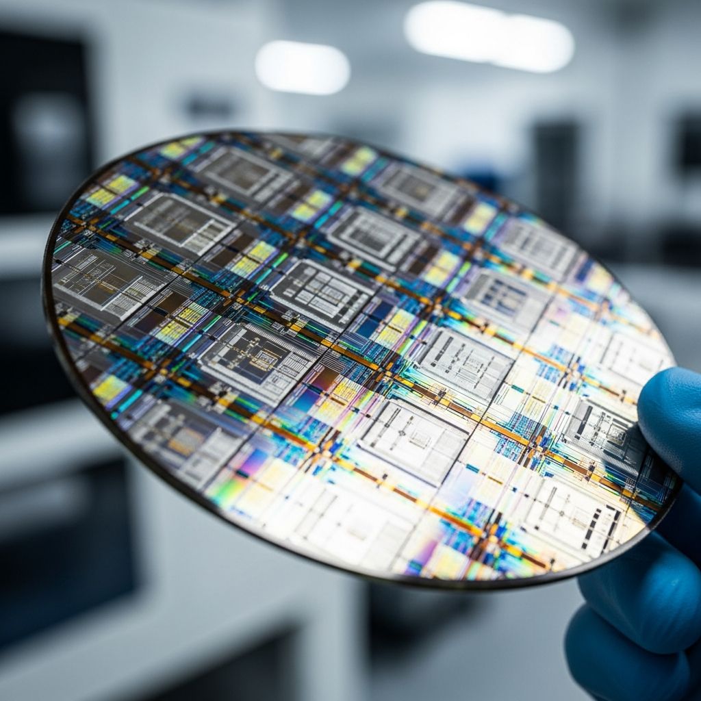
Semiconductors represent a cornerstone of contemporary technology, serving as materials with electrical conductivity positioned between that of conductors like metals and insulators like glass. This unique property allows precise control over electron flow, forming the basis for transistors, diodes, and integrated circuits that power devices from smartphones to supercomputers.
Core Principles of Semiconductor Materials
At their essence, semiconductors possess conductivity that can be tuned by external factors such as temperature, light, or impurities. Unlike pure conductors with free-moving electrons or insulators that block them entirely, semiconductors enable controlled switching, amplification, and signal processing essential for electronics.
Silicon dominates as the primary material due to its abundance—comprising about 28% of Earth’s crust—stability at high temperatures, and suitability for precise engineering. Other materials like germanium, gallium arsenide, silicon carbide, and gallium nitride offer specialized advantages for high-power, high-frequency, or optical uses.
How Doping Transforms Semiconductor Behavior
Pure semiconductors, or intrinsic types, exhibit limited conductivity. Introducing impurities through a process called doping creates n-type and p-type variants. In n-type, elements like phosphorus add extra electrons, enhancing negative charge carrier mobility. P-type doping with boron creates ‘holes’ or positive charge carriers by accepting electrons.
Combining n-type and p-type regions forms p-n junctions, the foundation of diodes and transistors. Voltage application across these junctions allows current to flow in one direction (forward bias) while blocking it in the reverse, enabling rectification and switching.
Key Doping Techniques
- Diffusion: Impurities spread into the crystal lattice at high temperatures for uniform distribution.
- Ion Implantation: Accelerated ions precisely embed dopants, ideal for modern nanoscale features.
- Epitaxial Growth: Layer-by-layer crystal building for high-purity junctions.
These methods achieve doping levels from 10^13 to 10^20 atoms per cubic centimeter, fine-tuning resistivity from insulating to conducting states.
From Wafers to Chips: The Fabrication Journey
Semiconductor manufacturing starts with ultra-pure silicon ingots grown via Czochralski process, sliced into 300mm wafers. Photolithography patterns circuits using UV light through masks, followed by etching, deposition, and doping to build multilayer structures.
Modern chips pack billions of transistors in areas smaller than a fingernail. A typical logic chip spans ~30 layers of interconnects, with transistors as small as 2nm enabling unprecedented density and speed per Moore’s Law, which predicts doubling of transistors every two years.
| Process Step | Description | Purpose |
|---|---|---|
| Wafer Preparation | Growing and polishing silicon ingots | Provide defect-free base |
| Photolithography | Exposing photoresist with light patterns | Define circuit features |
| Etching | Removing material selectively | Create 3D structures |
| Doping | Implanting impurities | Tune electrical properties |
| Deposition | Adding thin films (metals, insulators) | Build interconnects and gates |
| Testing & Dicing | Probing and cutting wafers | Yield functional chips |
This intricate process yields devices with power efficiency rivaling biological neurons, revolutionizing computation.
Essential Semiconductor Devices and Their Functions
Transistors: The Switching Heart
Invented in 1947, transistors amplify signals or act as switches. Field-effect transistors (FETs) like MOSFETs dominate, using electric fields to control channel conductivity without direct contact. Billions fit on a single chip, enabling logic gates for processors.
Diodes: One-Way Current Gates
Diodes permit current in one direction, vital for power supplies, LEDs, and signal demodulation. Schottky diodes offer ultra-fast switching for high-frequency apps, while Zener diodes regulate voltage precisely.
Integrated Circuits: Miniaturized Marvels
ICs combine thousands to trillions of components on silicon dies. Analog ICs handle continuous signals (amplifiers, sensors); digital ones process binary logic. System-on-Chip (SoC) integrates CPU, GPU, memory, and AI accelerators.
Semiconductors Powering Everyday and Emerging Tech
Consumer electronics rely on semiconductors for processing, memory (DRAM, NAND flash), and displays (OLED drivers). Smartphones boast multi-core SoCs running at GHz speeds with neural processing units for AI tasks like photography.
In automotive, silicon carbide MOSFETs manage EV powertrains, boosting efficiency by 10% and range significantly. GaN devices enable compact 5G base stations and fast chargers. Medical imaging uses specialized sensors for MRI and CT precision.
Clean energy benefits from power semiconductors in solar inverters and wind turbines, optimizing grid integration. Defense leverages radiation-hardened chips for satellites.
Challenges and the Path Forward
Shrinking transistors faces quantum limits: tunneling leaks current below 1nm. Solutions include 3D stacking (FinFETs, GAAFETs), new materials like 2D graphene, and chiplet architectures for modular scaling.
Supply chain vulnerabilities, highlighted by 2021 shortages, spur investments in domestic fabs. Quantum computing promises semiconductors beyond classical limits using superconducting materials.
Sustainability drives recycling of rare earth dopants and energy-efficient fabs, which consume vast electricity but enable global decarbonization via EVs and renewables.
Frequently Asked Questions (FAQs)
What makes a material a semiconductor?
A semiconductor has conductivity between conductors and insulators, modifiable by doping, temperature, or light to control electron flow precisely.
Why is silicon the top choice for chips?
Silicon’s abundance, thermal stability, and mature ecosystem allow reliable fabrication of complex, nanoscale devices.
How do transistors enable computing?
Transistors switch on/off billions of times per second, representing binary 1s and 0s to perform logic operations in CPUs and memory.
What new materials are replacing silicon?
GaN and SiC excel in power electronics for EVs; InP for photonics. These handle higher voltages and frequencies than silicon.
Will Moore’s Law continue?
Traditional scaling slows, but innovations like chiplets and AI-driven design sustain performance gains into the 2030s.
Global Impact and Future Horizons
The Fourth Industrial Revolution amplifies semiconductor demand as IoT connects 75 billion devices by 2025, each needing chips. AI training requires exaflop-scale accelerators, pushing HBM memory and optical interconnects.
Semiconductors underpin economic growth: the industry exceeds $500B annually, employing millions. Geopolitical shifts build resilient supply chains in the US, Europe, and Asia.
Looking ahead, neuromorphic chips mimic brains for efficient AI, while photonics replaces electrons for terahertz speeds. Semiconductors will propel humanity toward sustainable, intelligent futures.
References
- What is a semiconductor? — Nikon. 2023. https://www.nikon.com/business/semi/technology/story01.html
- What is a semiconductor? — McKinsey & Company. 2023-05-12. https://www.mckinsey.com/featured-insights/mckinsey-explainers/what-is-a-semiconductor
- What are Semiconductors? — Intel Newsroom. 2023-07-20. https://newsroom.intel.com/tech101/what-are-semiconductors
- Semiconductor — Wikipedia (informs primary sources). N/A. https://en.wikipedia.org/wiki/Semiconductor
- What is a Semiconductor? — Toshiba Electronic Devices & Storage. 2024. https://toshiba.semicon-storage.com/us/semiconductor/knowledge/e-learning/discrete/chap1/chap1-1.html
- What is a Semiconductor? — IBM. 2024-02-15. https://www.ibm.com/think/topics/semiconductors
- About Semiconductors — Semiconductor Industry Association. 2024. https://www.semiconductors.org/semiconductors-101/what-is-a-semiconductor/

Medha Deb is an editor with a master's degree in Applied Linguistics from the University of Hyderabad. She believes that her qualification has helped her develop a deep understanding of language and its application in various contexts. Medha specializes in the areas of beauty, health, sports, and wellness and is committed to ensuring that the content on the website is…